KiCAD | PCB Design
Exploring PCB design with KiCAD | Learning schematic capture, layout, and manufacturing for custom electronics project
Project Details / Background
As part of an ongoing personal project, I'm learning to design and simulate a custom PCB to strengthen my understanding of schematic capture, layout design, and circuit simulation. The board is intended for use in simple electronics or robotics applications. Learning KiCAD will serve as hands-on experience and practice in working with component libraries, routing strategies, and learning about design rules for manufacturing.
I am also completing a KiCAD PCB Design course on Udemy to build a strong foundation in professional board design workflows. The course covers schematic capture, multi-layer PCB layout and routing, complementing my project and preparing me for real-world PCB manufacturing processes.
Image Gallery
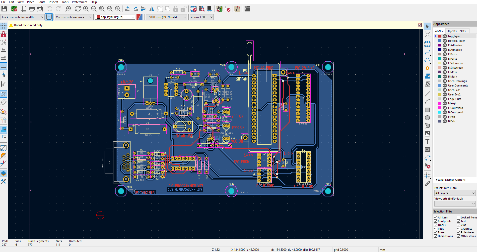 Practicing PCB layout with a KiCAD DEMO project.
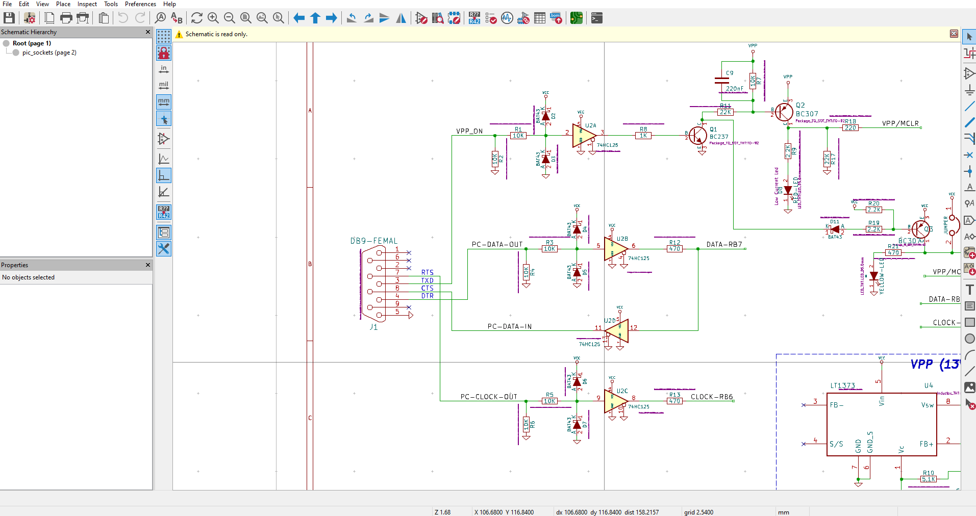 Schematic capture of the DEMO project. Learning multi-layer PCB design and routing strategies